Products

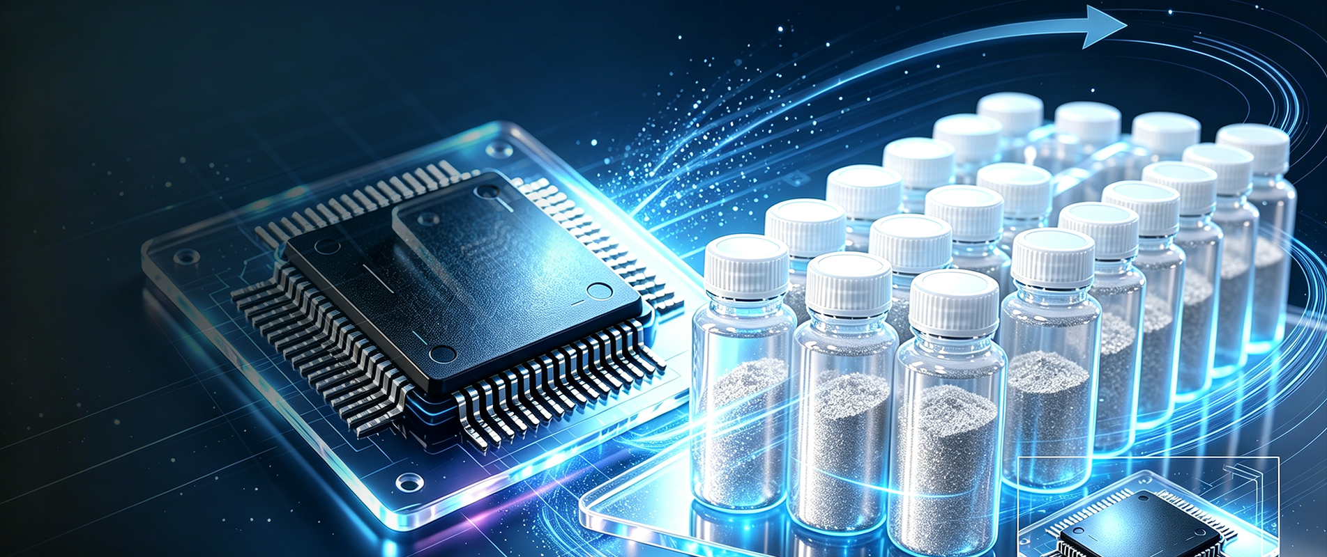
We Pioneer Boron Materials, Redefining Industrial Limits with Hong Kong-backed R&D and Ultra-high Purity Standards.
  • Elemental Boron

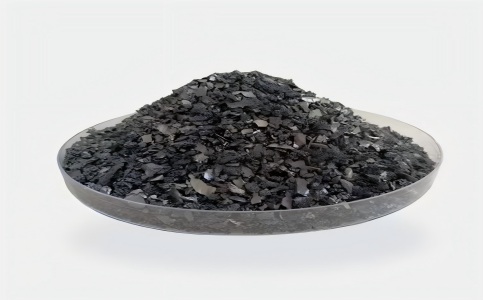
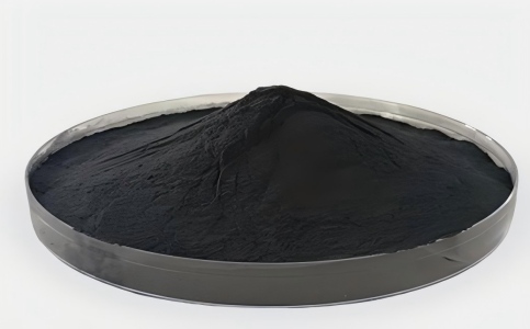
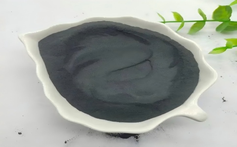
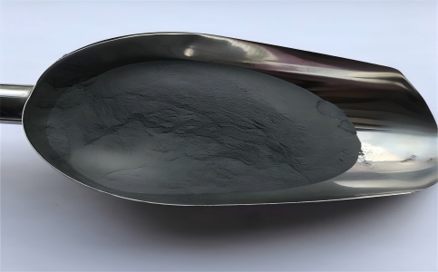
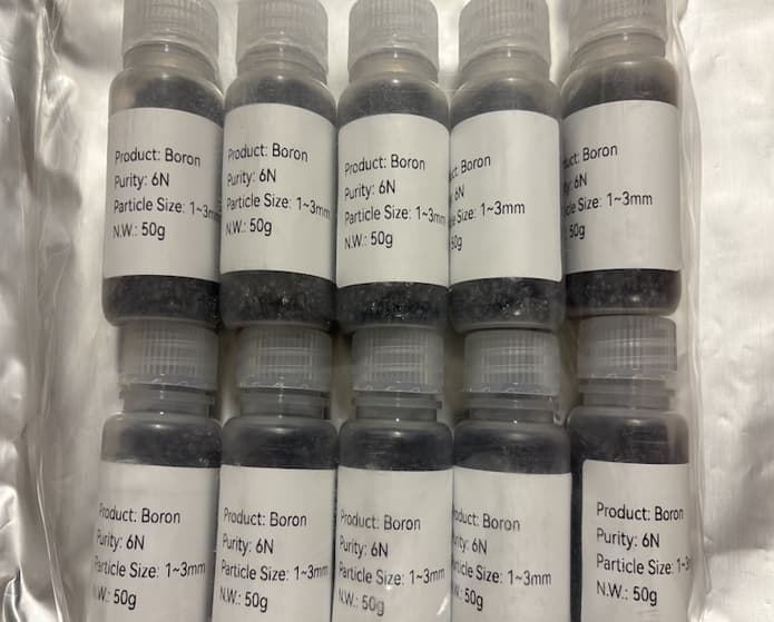
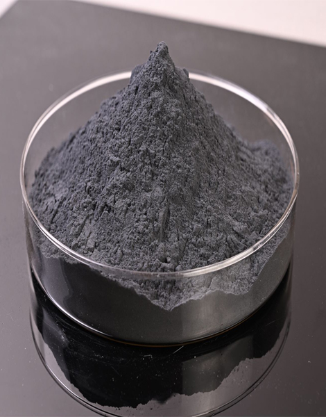
    Elemental Boron – Crystalline & Amorphous Elemental boron is the foundation of BoronHub’s portfolio, divided into high-purity crystalline boron and amorphous boron for distinct industrial applications.   High-Purity Crystalline Boron (4N–6N) β-rhombohedral structure, available as grey-brown powder (>500μm) or granules (1–10 mm), with purity from 99.99% (4N) to 99.9999% (6N). It offers exceptional chemical stability, Mohs hardness of 9.3, melting point of 2076 °C, and semiconductor properties. Used in silicon wafer doping, superhard material synthesis (e.g., CBN), aerospace alloys, and high-energy fuels.   Amorphous Boron (2N–3N) α-tetragonal short-range ordered structure, dark brown powder (>500μm). It is chemically reactive: oxidation starts at 300 °C, ignition at 700 °C, and it dissolves in concentrated alkalis with hydrogen release. Applications include rocket propellants, airbag initiators, alloy steels, boron fibers, and synthesis of boron halides and rare earth borides (e.g., LaB₆).   Customization BoronHub offers full flexibility across purity (2N–6N), particle size (submicron to 10 mm), and crystal form (α/β). Products are vacuum-sealed in aluminum foil bags or inert-gas PTFE bottles, 12-month shelf life. Tailored specifications available for semiconductor, nuclear, aerospace, metallurgy, and fine chemical industries.
    Explore More
  • Boron Isotopes

    Boron has two stable isotopes ¹⁰B and ¹¹B, with natural abundances of approximately 19.78% and 80.22% respectively. ¹⁰B features an extremely high thermal neutron capture cross-section, making it an outstanding neutron-absorbing material for nuclear power applications such as reactor power regulation and emergency shutdown systems. In contrast, ¹¹B barely absorbs neutrons and serves as a core material for semiconductor ion implantation.   BoronHub Offers a full portfolio of high-abundance boron isotopes with customizable enrichment levels to meet client specifications. Isotopic ¹⁰B exists as cubic β-type crystals with high purity and enrichment, and readily forms alloys with metals. Enriched boric acid-10 boasts a purity above 99.95 wt%, widely used as a soluble chemical shim in pressurized water reactors (PWRs). Enriched boron trifluoride-11 has a purity exceeding 99.999%, functioning as a critical p-type ion implantation dopant for the manufacturing of semiconductor chips and display panels.   All products are packaged in PTFE bottles filled with inert shielding gas. Customization of purity, isotope abundance and packaging specifications is available, supporting cutting-edge sectors including nuclear power, semiconductors, biomedicine and aerospace.
    Explore More
  • Boron Nitride

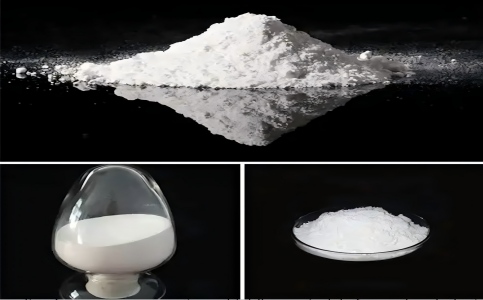
    Boron Nitride Product Classification Introduction Boron nitride (BN) is a premium functional boron-based material with an extremely versatile set of properties. BoronHub offers two core product lines: hexagonal boron nitride (h-BN) and cubic boron nitride (CBN), serving multiple high-end industries such as lubrication, thermal management and superhard precision machining.   Hexagonal Boron Nitride (h-BN) Nicknamed "white graphite", h-BN is pure white powder that integrates excellent high-temperature lubricity, high thermal conductivity, superior electrical insulation, chemical inertness and strong neutron absorption capacity. BoronHub supplies customized flaky h-BN powder with high purity and high crystallinity, with particle sizes reducible to less than 1 μm. Its typical application scenarios include high-temperature release agents, chip thermal interface materials, aerospace wave-transparent composites, neutron shielding materials for nuclear power, and functional fillers for luxury cosmetics.   Cubic Boron Nitride (CBN) CBN is a superhard material whose hardness is second only to diamond. Its wear resistance exceeds that of conventional abrasives by over four times, paired with outstanding thermal stability and chemical inertness, making it perfectly suited for high-precision grinding of ferrous metals and their alloys. BoronHub provides single-crystal CBN (HBCBN series, Ti hardness index: 63–76) and CBN micropowder (12 grades with D50 ranging from 1.25 μm to 32 μm) compatible with all types of binder systems. It is widely used in CBN grinding wheels, PCBN cutting tools, automotive component precision machining and heat dissipation for electronic packaging.   Supported by high purity, exceptional thermal stability, a full spectrum of particle sizes and flexible customization services, BoronHub delivers comprehensive boron nitride material solutions for global clients.  
    Explore More
  • Boron Carbide

    Also nicknamed "black diamond", boron carbide ranks among the three hardest known materials, with hardness second only to diamond and cubic boron nitride (CBN). It features an ultra-low density of 2.52 g/cm³, a high melting point of 2450 °C, and outstanding chemical stability, remaining inert to both strong acids and strong alkalis.   The core advantage of boron carbide lies in its exceptional neutron absorption capacity. Boron elements possess a large neutron capture cross-section, which enables efficient thermal neutron absorption without generating long-lived radionuclides. This property makes boron carbide an essential material for nuclear reactor control rods, radiation shielding and spent fuel storage applications.   Meanwhile, benefiting from its lightweight and high-strength characteristics, boron carbide is widely adopted in protection fields such as ballistic armor and individual armor inserts. For industrial applications, it serves as a superhard abrasive for grinding and polishing cemented carbides and gemstones, as well as for manufacturing precision components including high-wear nozzles and sealing rings.   BoronHub supplies high-purity boron carbide powder with customizable particle sizes to meet diverse application requirements across nuclear industry, high-end ballistic protection, precision machining and refractory materials.  
    Explore More
  • Rare Earth Hexaborides

    Rare earth hexaborides (general formula: REB₆) are a family of functional ceramic materials with cubic crystal structures. Featuring low work function, high electron emissivity, high melting point and excellent thermal stability, they serve as core materials for advanced electron emission applications.   BoronHub offers two flagship products: lanthanum hexaboride (LaB₆) and cerium hexaboride (CeB₆), both with purity above 99.9%. Multiple forms are available including nanopowders and single-crystal granules.   Lanthanum Hexaboride (LaB₆) LaB₆ has a work function of approximately 2.5–2.7 eV, delivering high emission brightness and stable beam current. It is the preferred thermocathode material for scanning electron microscopes (SEM), transmission electron microscopes (TEM), electron beam lithography systems and particle accelerators. Single-crystal LaB₆ cathodes achieve over 10 times the brightness of tungsten cathodes, and are widely deployed in electron optics, aerospace and high-end scientific research.   Cerium Hexaboride (CeB₆) CeB₆ exhibits superior resistance to carbon contamination, with a service life 50% longer than LaB₆. It features a lower evaporation rate at 1700 K, making it suitable for long-lifetime, high-stability applications such as microwave tubes, electron beam welding equipment, X-ray tubes and free-electron lasers.   BoronHub supplies high-purity LaB₆ and CeB₆ with customizable particle sizes, fully supporting industries covering electron optics, semiconductor equipment, aerospace and cutting-edge scientific research.  
    Explore More
  • Transition Metal Borides

    Transition metal borides (TMBs) are intermetallic compounds formed by transition metal elements (such as Ti, Zr, Hf, Mg, etc.) bonded with boron atoms. They combine the high hardness and high melting point of ceramics with the excellent electrical and thermal conductivity of metals. These materials generally feature ultra-high melting points (some exceeding 3000 °C), exceptional hardness, superior wear resistance, corrosion resistance and high-temperature stability, presenting broad application prospects in superhard materials, ultra-high-temperature ceramics, catalysts and electronics.   BoronHub custom-develops the following transition metal boride products: Magnesium diboride (MgB₂) is a high-temperature superconductor with a critical temperature of approximately 39 K, with significant applications in superconducting magnets, MRI systems, power transmission and superconducting electronic devices. Hafnium diboride (HfB₂), with a melting point as high as 3380 °C, is one of the core materials of ultra-high-temperature ceramics (UHTCs). It is used for extreme high-temperature components such as thermal protection systems of hypersonic vehicles, nose cones, wing leading edges and engine nozzles. Zirconium diboride (ZrB₂), with a melting point of approximately 3245 °C, also belongs to the ultra-high-temperature ceramic family. It is deployed in scenarios including thermal protection for hypersonic vehicles, re-entry vehicles and crucibles for molten metals.   BoronHub provides stable supply of high-purity transition metal boride powders with customizable particle sizes, fully serving the global high-end manufacturing sector across cutting-edge fields including aerospace, superconducting technology, superhard materials and high-temperature structural ceramics.  
    Explore More
About Us

We Unlock Boron’s Power As the Global Hub of Ultra-pure Boron Material Solutions

BoronHub Solutions Limited is a technology-oriented enterprise specializing in R&D, custom manufacturing and global supply of high-end boron-based new materials. Centered on two core strategic product lines – ultra-high-purity elemental boron and customized boron isotopes, we supply a full spectrum of borides including hexagonal boron nitride, cubic boron nitride, boron carbide, rare earth hexaborides and transition metal borides. We have built a complete industrial chain system covering core raw materials, functional borides and customized industrial solutions, serving high-precision manufacturing sectors worldwide such as semiconductors, BNCT nuclear medicine, civil nuclear power, commercial aerospace and new energy. Rooted in self-developed and fully controllable core separation and purification technologies, BoronHub strives to be a trusted integrated partner for high-end boron materials across the globe.
Learn More about BORONHUB

Technical Document Download Center

Latest complete technical documentation suite for boron products, including COAs, TDSs, MSDSs and compliance declarations, available for your download and review as supporting references for procurement, quality inspection and safe material application.
View / Download Documents
Industries We Serve

Custom Boron From 2N to 6N Plus Tailored Isotopes For Semiconductor, Civilian Nuclear And Aerospace Cutting-edge Industries.

Ultra-High Purity Dopant for Semiconductor Monocrystalline Silicon Crystal Pulling

Target Customers: Wafer fabs, monocrystalline silicon crystal growers, semiconductor equipment manufacturers   6N High-Purity Crystalline Boron (99.9999%) – Core Product   Detailed Applications High-purity boron is known as the "vitamin of industry", with its major applications concentrated in three strategically important industrial sectors: semiconductors, aerospace and nuclear power. High-purity silicon itself acts as an insulator; boron doping is mandatory to convert it into stable semiconducting material for high-end chip fabrication. Ultra-high-purity 6N crystalline boron serves as the primary P-type dopant for monocrystalline silicon ingot pulling via Czochralski (CZ) and Float Zone (FZ) techniques, functioning as a critical material governing wafer resistivity uniformity and carrier mobility. Its extreme 6N purity prevents contamination by detrimental heavy metals such as iron and copper during doping, which directly defines the electrical performance consistency and carrier transport efficiency of finished wafers. The sophisticated manufacturing processes and proprietary technology required for boron production once made this material a bottleneck restricting the development of the semiconductor industry, as well as leverage for international sanctions.    Through years of joint R&D collaboration with renowned universities in Hong Kong and mainland China, we have fully mastered independent mass production technology for 6N crystalline boron. Our product technical specifications and stable supply capacity can fully satisfy application demands from semiconductor manufacturers worldwide. Currently, more than 85% of monocrystalline silicon wafers globally are produced by the Czochralski method. P-type silicon wafer manufacturing represents the most mature process route, generating sustained rigid demand for high-purity boron dopants. 6N crystalline boron acts as an irreplaceable core doping source for silicon substrates used in logic chips and memory devices, FZ monocrystalline silicon for power semiconductors (IGBTs, MOSFETs), and P-type monocrystalline silicon wafers for photovoltaic applications.  

Explore the Industries

Semiconductors, Advanced Chips & Third-Generation Semiconductors

Semiconductors, Advanced Chips & Third-Generation Semiconductors Target Clients: Wafer fabs (TSMC, SMIC, etc.), monocrystalline silicon/silicon carbide crystal growers, thermal management manufacturers for AI servers, semiconductor equipment suppliers 6N High-Purity Crystalline Boron (99.9999%) – Core Product Application: Serves as the primary P-type dopant for monocrystalline silicon ingot pulling via Czochralski (CZ) and Float Zone (FZ) methods. Its ultra-high 6N purity avoids harmful heavy metal contaminants such as iron and copper during silicon crystal growth, directly guaranteeing uniform wafer resistivity and carrier mobility. Isotope-Enriched Boron-11 (Elemental Form / High-Purity Enriched Grade) Application: Wafer doping for advanced process nodes of 3 nm and below, as well as modification of SiC/GaN wide-bandgap power devices. Since boron-11 does not absorb neutrons, it effectively eliminates chip soft errors triggered by neutron irradiation and enhances radiation resistance and reliability for high-end AI chips and aerospace-grade semiconductors. Enriched Boron Trifluoride-11 (¹¹BF₃) – New Flagship Product Application: Gas-phase ion implantation dopant for front-end semiconductor manufacturing (to fabricate high-performance P-type semiconductors), and Lewis acid catalyst for advanced organic synthesis. High-Purity Nano-Scale Hexagonal Boron Nitride (h-BN) Application: Thermal interface material (TIM) thermal filler/thermal pads for core chips in AI servers, insulating heat dissipation layers for high-power electronic devices. Cubic Boron Nitride (c-BN) Micropowder Application: Ultra-precision polishing of third-generation power wafers including silicon carbide (SiC), and superabrasives for micro-drills in high-end PCBs. Lanthanum Hexaboride (LaB₆) Application: Cathode material for plasma electron guns in semiconductor etching equipment, electron emission sources for high-end vacuum coating systems.  

Explore the Industries
Biomedicine & Advanced Nuclear Medicine (BNCT Tumor Therapy)

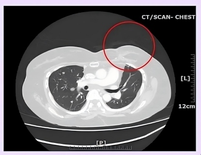
Biomedicine & Advanced Nuclear Medicine (BNCT Tumor Therapy) Target Clients: Nuclear drug R&D enterprises, BNCT centers in oncology hospitals, biomedical research institutes Enriched Boric Acid-10 Application: Synthesizes boron-targeted delivery agents for BNCT tumor therapy (e.g., BPA, BSH), functioning as the key upstream precursor raw material for boron neutron capture therapy pharmaceuticals. Isotope-Enriched Boron-10 (Customizable Elemental/Compound Forms) Application: Core boron source for clinical BNCT agents. It accumulates selectively within tumor cells and, upon bombardment by external neutron beams, precisely destroys cancerous cells.

Explore the Industries

Nuclear Power, Nuclear Industry & Neutron Shielding

Nuclear Power, Nuclear Industry & Neutron Shielding Target Clients: Nuclear power equipment manufacturers, research institutes of CGN & CNNC, semiconductor irradiation facilities, nuclear detection instrument vendors Isotope-Enriched Boron-10 Application: Fabrication of nuclear reactor control rods and radiation shielding panels. It efficiently captures thermal neutrons to regulate nuclear reaction power, and also provides neutron shielding for semiconductor irradiation processes. Boron Carbide (B₄C) Application: Neutron shielding blocks and reactor core pellets for nuclear power plants, serving as lightweight core structural components for neutron absorption and radiation protection. Hafnium Diboride (HfB₂) Application: Combines superior neutron absorption capacity and corrosion resistance; used as erosion-resistant lining coatings for nuclear reactor interiors and protective cladding for nuclear fuels. Enriched Boron Trifluoride-11 (¹¹BF₃) – New Flagship Product Application: Isotope calibration in nuclear research, low-interference nuclear detection reagents, and working mediums for high-performance neutron counters/gas detectors.

Explore the Industries

Aerospace, Special Propellants & National Defense

 Aerospace, Special Propellants & National Defense Target Clients: Aerospace propellant research institutes, solid rocket motor manufacturers, military ballistic protection equipment producers 3N Amorphous Boron Powder (99.9%) – New Flagship Product Application: High-energy additive for solid rocket propellants, pyrotechnics and igniters. Amorphous boron powder features extremely high mass calorific value (roughly twice that of carbon) and low density, significantly boosting thrust and specific impulse of rockets and missiles. It also acts as the core initiator in gas generants for automotive airbags. Boron Carbide (B₄C) Application: Lightweight ballistic inserts for individual soldiers and lightweight protective armor for armed helicopters & armored vehicles, balancing ultra-light weight with outstanding bulletproof performance. Hafnium Diboride (HfB₂) Application: Ultra-high temperature thermal protection coatings (UHTCs) for leading edges of hypersonic vehicles, throat liners for rocket nozzles and other extreme-temperature erosion-resistant components. Zirconium Diboride (ZrB₂) Application: High-temperature thermal insulation coatings for aircraft, high-temperature metallurgical electrodes for aerospace applications. Hexagonal Boron Nitride (h-BN) Application: High-temperature insulation and ablation-resistant structural parts for thermal protection and propulsion systems of aerospace vehicles.

Explore the Industries

New Energy Industry (Power Batteries, Energy Storage, Aluminum Electrolysis & Lightweighting)

New Energy Industry (Power Batteries, Energy Storage, Aluminum Electrolysis & Lightweighting) Target Clients: Major lithium battery manufacturers, aluminum smelters, new energy vehicle OEMs & component suppliers Nano-Scale Hexagonal Boron Nitride (h-BN) Powder Application: High-temperature resistant coating on lithium battery separators to effectively inhibit thermal runaway; thermal conductive filler for energy storage converters. Titanium Diboride (TiB₂) Application: Wettable inert cathode material for aluminum electrolytic cells, drastically cutting power consumption of aluminum smelting and extending cell service life. Copper Boron Alloy (CuB) Application: Alloy modification additive for high-power copper busbars in energy storage and lead frames of new energy vehicles, improving copper strength and heat resistance. Aluminum Diboride (AlB₂) Application: Reinforcing particles for lightweight structural components such as automotive aluminum alloy wheel hubs and chassis, enhancing wear resistance and rigidity of aluminum matrix composites. Ferroboron Alloy (FeB, 17–20% Boron Content) Application: Micro-alloying modifier for high-strength gear steel and bearing steel in new energy vehicles, elevating steel hardenability.

Explore the Industries
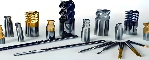
High-Precision Machining, Special Cutting Tools & Surface Engineering

High-Precision Machining, Special Cutting Tools & Surface Engineering Target Clients: Superhard tool manufacturers, precision mold makers, photovoltaic silicon wafer processors, PVD/CVD coating enterprises 3N Amorphous Boron Powder Application: High-activity boronizing agent for surface treatment of specialty alloys, forming an ultra-hard boride layer on workpiece surfaces and exponentially boosting wear resistance of mechanical components. Cubic Boron Nitride (c-BN) Single Crystals / Micropowder Application: Fabrication of superhard cutting tools for precision machining and grinding of hard-to-cut ferrous metals including quenched steel, high-temperature alloys and new energy vehicle transmission parts. Boron Carbide (B₄C) Application: Cutting abrasives for large-size photovoltaic silicon ingots, ultra-precision lapping and polishing media for sapphire substrates and semiconductor wafers. Titanium Diboride (TiB₂) / Chromium Diboride (CrB₂) Application: Wear-resistant PVD coatings for industrial cutting tools, anti-corrosion & wear-resistant coatings on precision tooling surfaces.

Explore the Industries
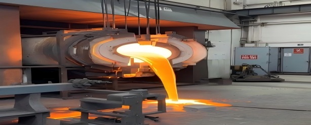
Metallurgy, Special Glass & Refractory Materials

Metallurgy, Special Glass & Refractory Materials Target Clients: Special steel mills, non-ferrous metal smelters, premium specialty glass manufacturers (fiber drawing & optoelectronic glass) Ferroboron Alloy (FeB, 17–20% Boron Content) Application: Deoxidizer and grain refiner for smelting high-strength structural steel, heavy-load bearing steel and permanent magnet steel, greatly improving steel hardenability. Zirconium Diboride (ZrB₂) Application: High-temperature refractory molds for glass fiber forming and high-temperature electrodes for specialty glass production, featuring exceptional oxidation resistance and resistance to erosion by molten metallurgical materials. Full Range of Pre-Alloyed Boron Powders (FeB / NiB / CuB / ZrB / MoB / CoB) Application: Modification additives for high-end non-ferrous & specialty alloy smelting, or raw materials for powder metallurgy forming. Custom boron content and precise particle size distribution available on demand.

Explore the Industries
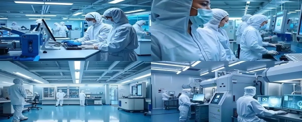
Advanced Miscellaneous Applications (Scientific Instruments / Superconductors / Cosmetics / Fine Chemicals)

Advanced Miscellaneous Applications (Scientific Instruments / Superconductors / Cosmetics / Fine Chemicals) Lanthanum Hexaboride (LaB₆) / Cerium Hexaboride (CeB₆) Application: Cathode materials for electron guns in transmission electron microscopes (TEM) and scanning electron microscopes (SEM), high-temperature long-life electron cathodes for deep space probes. Magnesium Diboride (MgB₂) Application: Commercially viable mid-temperature superconducting material, used to fabricate low-cost superconducting magnet coils for medical MRI scanners and urban superconducting power transmission cables. Ultra-Fine High-Purity Hexagonal Boron Nitride (h-BN) Powder Application: Premium matte powder for high-end cosmetics (compacts, eyeshadows, etc.), delivering silky texture and natural coverage.

Explore the Industries

FAQ: Quick and Clear Answers to Your Key Questions.

BoronHub is a technology-driven advanced materials enterprise. We are headquartered in Hong Kong with operational offices in Shenzhen and compliant production bases located in mainland China. We independently master core technologies for high-purity boron purification and boron isotope separation, a...
Our core product lines fall into two major groups: * High-purity elemental boron (6N crystalline boron, 3N amorphous boron); * Full-spectrum boron isotopes (elemental ¹⁰B, elemental ¹¹B, enriched boric acid-¹⁰B, enriched boric acid-¹¹B, enriched boron trifluoride-¹...
Raw materials are sourced from compliant salt-lake boron ore bases within China with full traceability across the supply chain. We maintain sufficient production capacity to fulfill stable bulk orders for global clients over the long term.
Every product corresponds to an official CAS registry number, e.g. crystalline boron CAS 7440-42-8, boron carbide CAS 12069-32-8. CAS documentation can be provided alongside orders for customers’ qualification filings.
Our domestic manufacturing facilities are confidential units filed with government authorities under strict site access control, and are not open to external tours or on-site inspections. We apologize for any inconvenience this may cause. Complete quality inspection and compliance documents can be p...
If your questions remain unanswered, please contact our technical sales team for one-on-one consultation.
This FAQ library streamlines communication and resolves common inquiries on product selection, technical specs, export compliance, and order procedures. Content is based on actual specifications and regulations to build trust for cooperation.

Blog and media

BLOG
News
Testing Methods Determine Boron Material Grades
Aug 15,2026

Testing Methods Determine Boron Material Grades

Testing Methods Determine Material Grades: Methodological Differences in Particle Size and Purity Testing of Boron-Based Materials Introduction In the international procurement of boron-based materials, purchasing engineers frequently encounter a confusing phenomenon: identical batches of boron materials yield drastically different test results when examined via disparate testing protocols. Particle size readings can shift from "non-compliant" to "qualified", while purity grades may swing from 6N to 4N. This raises a critical question: are these discrepancies caused by the material itself, or by the testing methodologies employed? Drawing on two real-world testing cases, this paper analyzes the gaps between Scanning Electron Microscopy (SEM) and laser particle size analyzers for particle size measurement, as well as the divergent outputs of ICP-MS and GDMS purity testing. It aims to help customers establish rigorous testing awareness and avoid flawed procurement judgments stemming from misinterpreted test data.   I. Particle Size Testing: Why SEM and Laser Particle Size Analyzer Deliver Contradictory Results 1. Case Study: 2–4 μm Boron Powder Misjudged by SEM A South Korean client purchased amorphous boron powder with a contractual particle size specification of 2–4 μm. When inspected under a Scanning Electron Microscope (SEM), severe particle agglomeration was observed, leading the client to deem the product non-conforming. However, re-testing conducted by BoronHub using a laser particle size analyzer, with standard pre-treatment including sodium pyrophosphate dispersant and ultrasonic de-agglomeration, produced D50 values fully within the 2–4 μm target range, confirming the product meets specifications. Why do two testing techniques produce opposing conclusions for the same batch of material?   2. Fundamental Principle Differences: Visual Imaging vs. Statistical Distribution Scanning Electron Microscopy (SEM) SEM scans the sample surface with a focused high-energy electron beam to generate high-resolution morphological images. It enables direct observation of particle shape, surface structure and agglomeration status, making it invaluable for material R&D and morphological analysis. Nevertheless, it carries notable limitations:   No capacity for full distribution statistics: SEM only captures several hundred particles within a limited field of view, which cannot represent the true particle size distribution of an entire powder batch.   High risk of agglomeration misjudgment: For readily agglomerated boron powder, SEM imagery confuses agglomerates with large primary particles and cannot distinguish genuine coarse grains from clustered particles.   Substantial quantitative error: Measurement deviations for primary particles via SEM can reach 15%–30%.     Laser Particle Size Analyzer This instrument operates on laser diffraction principles (ISO 13320:2020). As particles pass through a laser beam, light scattering occurs; the device calculates volumetric particle size distribution based on the angle and intensity of scattered light. As a statistical testing technique, it rapidly and accurately characterizes the overall particle size distribution of a sample, outputting critical metrics including D10, D50 and D90. Within the elemental boron industry, laser particle size analysis is the standard routine testing method and globally accepted acceptance criterion.   3. Core Conclusion SEM captures the morphology of individual particles, while laser particle size analyzers generate statistical distribution data for the bulk powder population. For boron powder used in semiconductor doping, production processes prioritize consistent overall particle size distribution (quantified via D10, D50, D90) rather than the morphology of isolated particles. Accordingly, laser particle size analysis complying with ISO 13320:2020 is the internationally recognized standard for particle size acceptance testing. SEM is only suitable for morphological observation and shall not be used as a basis for batch rejection.   4. Practical Guidance for Buyers Clarify acceptance metrics: Require suppliers to provide D10, D50 and D90 data instead of vague "XX micron" specifications. Specify testing methodology: Explicitly designate laser particle size analysis (ISO 13320) as the sole acceptance standard within contracts or specification sheets. Verify pre-treatment protocols: Confirm the use of dispersants and ultrasonic de-agglomeration standard pre-treatment for agglomeration-prone powders. Treat SEM as auxiliary only: SEM may be used for morphological and agglomeration observation but cannot independently justify product rejection.   II. Purity Testing: Discrepancies Between ICP-MS and GDMS Grading 1. Case Study: 6N or 4N? Determined by Test Element Scope A batch of 6N crystalline boron recorded total concentrations of 11 key impurities below 1 ppm via ICP-MS testing, corresponding to a stated purity of 99.9999% (6N). Yet identical material analyzed via GDMS detected over 70 impurity elements with a total impurity concentration exceeding 10 ppm, equating to a purity grade of only 99.99% (4N). The material composition remains unchanged, yet its purity rating drops drastically—what accounts for this disparity?   2. ICP-MS: Globally Accepted Standard for 6N Certification in the Semiconductor Industry Within the high-purity elemental boron sector, 6N purity classification is defined by ICP-MS testing of a defined set of critical impurity elements, rather than full-spectrum elemental screening. Below are the standard ICP-MS test specifications for BoronHub’s 6N crystalline boron: Element Specification Limit Test Method Al ≤ 0.4 ppm ICP-MS As ≤ 0.5 ppm ICP-MS Cr ≤ 0.2 ppm ICP-MS Cu ≤ 0.3 ppm ICP-MS Fe ≤ 0.9 ppm ICP-MS k ≤ 0.7 ppm ICP-MS Mg ≤ 0.5 ppm ICP-MS Na ≤ 0.5 ppm ICP-MS Ni ≤ 0.1 ppm ICP-MS Pb ≤ 0.1 ppm ICP-MS Sb ≤ 0.1 ppm ICP-MS Total Impurities < 1.0 ppm -   Inductively Coupled Plasma Mass Spectrometry (ICP-MS) uses liquid sample injection to precisely quantify heavy metal impurities hazardous to semiconductor devices (e.g., Fe, Cu, Ni, Pb). Material with total concentrations of these specified impurities below 1 ppm qualifies as 6N purity—this is the universal acceptance standard adopted by semiconductor wafer fabs worldwide.   3. GDMS: Comprehensive Full-Spectrum Element Screening Tool Glow Discharge Mass Spectrometry (GDMS) enables direct solid sample analysis and detects up to 70 impurity elements spanning nearly the entire periodic table, including alkali metals, rare earths and non-metallic contaminants.   GDMS screens a far broader range of impurities than ICP-MS. Even with each individual impurity present at ultra-low concentrations, cumulative total impurity levels will inevitably rise, which may reduce the calculated purity to 4N when accounting for all trace elements. This does not indicate inferior material quality—the chemical composition remains identical; only the statistical scope differs.   ICP-MS quantifies concentrations of predefined harmful elements to validate compliance with 6N grading. GDMS delivers a full elemental impurity profile for research traceability and comprehensive material characterization.     4. Functional Division and Positioning of the Two Testing Methods Comparison Item ICP-MS GDMS Sample Injection Mode Liquid injection (sample dissolution required) Direct solid injection Detected Elements 11 key semiconductor-hazardous impurities Up to 70 elements (full-spectrum screening) Detection Limit ppb level ppb level Industrial Application Universal standard for 6N purity certification Full-element traceability & R&D analysis Applicable Scenarios Factory release testing, incoming material inspection Material research, anomaly troubleshooting   5. Practical Guidance for Buyers Define 6N clearly: 6N grading refers to total concentrations of the specified 11 critical impurities below 1 ppm, not full-spectrum elemental purity. Request complete test reports: Demand numerical measured values (ppm/ppb) for each element instead of merely a "6N" label. Standardize acceptance methodology: Adopt ICP-MS as the benchmark for batch acceptance, consistent with industry-wide 6N grading norms. Deploy GDMS for R&D purposes: Request supplementary GDMS full-element analysis reports for research or anomaly investigation if required.   III. Complete Practical Operation Manual for Purchasers and Engineers 5-Step Particle Size Testing Protocol Step Core Requirements 1. Clarify Metrics Require D10, D50, D90 data instead of vague micron-range descriptions 2. Specify Test Method Contractually designate laser particle size analysis (ISO 13320) as the sole acceptance standard 3. Confirm Pre-Treatment Verify dispersant type (e.g., sodium pyrophosphate), ultrasonic duration and dispersion parameters 4. Request Distribution Curves Demand full particle size distribution plots, not isolated single numerical values 5. Restrict SEM to Reference Use SEM serves only morphological observation and cannot act as particle size acceptance criteria   4-Step Purity Testing Protocol Step Core Requirements 1. Understand 6N Definition 6N grading relies on ICP-MS testing of 11 predefined critical impurities, not full-spectrum elemental analysis 2. Confirm Test Benchmark Acceptance testing shall reference ICP-MS; GDMS is reserved for full-element traceability 3. Obtain Full Quantitative Data Request individual element readings and total impurity content, not just percentage purity values 4. Demand Original COA Documentation Reports must specify testing instruments, methodologies, detection limits and individual element concentrations   IV. BoronHub’s Testing Standards and Commitments As a professional supplier of advanced boron-based materials, BoronHub adheres to the strictest international testing standards:   1.Particle Size Testing: Laser particle size analyzers compliant with ISO 13320:2020, paired with standardized pre-treatment (sodium pyrophosphate dispersion + ultrasonic de-agglomeration), ensuring repeatable, internationally comparable particle size data.   2.Purity Testing: Every batch of 6N-grade material undergoes ICP-MS analysis for 11 key impurities with total aggregate levels below 1 ppm, accompanied by complete COA documentation. GDMS full-element analysis reports are available upon customer request for R&D reference.   3.Transparency Commitment: All reports clearly disclose testing methodologies, the scope of analyzed elements and individual measured values to eliminate ambiguous labeling.   4.Traceable Data: All test certificates document testing protocols, detection limits and reference standards, with full traceability back to batch production records   Conclusion The choice between SEM and laser particle size analysis, or ICP-MS and GDMS, ultimately hinges on how manufacturers and buyers define "conforming material". Identical raw materials can yield vastly different test outcomes under divergent analytical methods—this is not material inconsistency, but a limitation inherent to each testing technique. Within the boron materials sector, laser particle size analysis is the universal particle size testing benchmark, while targeted ICP-MS impurity testing constitutes the industry standard for 6N purity certification. Sound procurement decisions are built upon a thorough understanding of testing methodologies. When partnering with BoronHub, customers receive not only high-purity boron materials, but also a fully traceable, verifiable and robust quality assurance framework. BoronHub – Defining High-Purity Boron Quality Through Scientific Testing To obtain specification sheets (TDS/COA) for 6N boron products or enquire about testing methodology details, please contact our technical team.      
Semiconductor-Grade Boron Trichloride Market Analysis Report
Aug 16,2026

Semiconductor-Grade Boron Trichloride Market Analysis Report

Surge in Demand for Semiconductor-Grade Boron Trichloride to Reach XXX Million; Projected XX% CAGR During 2025–2033 Forecast Period Market segmentation of semiconductor-grade boron trichloride covers application (diffusion doping, ion implantation, dry etching), purity grade (5N, 6N), and geographic regions including North America (US, Canada, Mexico), South America (Brazil, Argentina, Rest of South America), Europe (UK, Germany, France, Italy, Spain, Russia, Benelux, Nordic Countries, Rest of Europe), Middle East & Africa (Turkey, Israel, GCC, North Africa, South Africa, Rest of MEA), and Asia Pacific (China, India, Japan, South Korea, ASEAN, Oceania, Rest of APAC), with forecasts spanning 2026–2034.   By Khageshwar Rongkali, MRA | May 15, 2026   Key Insights The semiconductor industry’s relentless pursuit of miniaturization and high performance fuels robust demand for ultra-high-purity chemicals such as semiconductor-grade boron trichloride (BCl₃). The market is projected to hit USD 500 million by 2025 and maintain strong growth, driven by widening adoption of BCl₃ in the manufacturing of advanced semiconductors and related components. A compound annual growth rate (CAGR) of 7% is expected from 2025 to 2033, pushing the total market size to approximately USD 900 million by 2033.   Core growth drivers include booming 5G infrastructure rollout, the rise of high-performance computing (HPC), and mass adoption of advanced semiconductor nodes at 3nm and below. Additionally, the global shift to electric vehicles (EVs) and proliferation of the Internet of Things (IoT) further underpin market expansion. While supply chain bottlenecks and volatile raw material prices pose moderate restraints, long-term positive outlooks for the semiconductor sector sustain overall market optimism. Major global manufacturers are aggressively ramping up production capacity and advancing technical innovation to meet surging end-user demand.   The semiconductor-grade BCl₃ market is segmented primarily by purity, application (dopant, etchant) and geography. North America and Asia Pacific are forecast to dominate global consumption, supported by concentrated semiconductor fabrication capacity across both regions. Market competition is set to intensify as players strive to deliver high-purity, efficient, cost-effective products. Growing industry focus on sustainability and carbon footprint reduction accelerates the development of eco-friendly manufacturing workflows and waste management solutions within the BCl₃ supply chain. Continuous breakthroughs in semiconductor fabrication technology will reshape market dynamics over the coming years, bringing both opportunities and challenges to industry participants.   Concentration & Properties of Semiconductor-Grade Boron Trichloride Semiconductor-grade BCl₃ features purity exceeding 99.999%, a critical specification for wafer manufacturing workflows. Its commercial grade is defined by trace impurity thresholds, including silicon tetrachloride, boron tribromide and other halide contaminants. Even ppm-level trace impurities can severely degrade finished chip quality. Annual global output of semiconductor-grade BCl₃ stands at millions of metric tons, with the total market valued at hundreds of millions of US dollars.   Core Production Hub: East Asia (China, Japan, South Korea) accounts for the majority of global BCl₃ output, backed by dense concentration of semiconductor fabs. North America and Europe hold moderate yet smaller production shares.   Technical Innovation Focus: Current R&D priorities include advanced purification techniques to achieve ultra-high purity benchmarks, lower production expenses, and boost process safety, with innovative distillation and chemical refining methods under active development.     Regulatory Impacts: Stringent environmental regulations govern BCl₃ handling and disposal due to its high reactivity and toxic properties, inflating manufacturing and logistics costs and pushing enterprises to upgrade safety protocols and waste treatment systems. Product Substitutes: No direct chemical replacement exists for BCl₃ across mainstream semiconductor applications; emerging alternative doping technologies lack cost competitiveness and equivalent performance for full-scale fab deployment. End-User Concentration: Demand is highly consolidated among top-tier semiconductor manufacturers, with a handful of leading fabs accounting for the majority of global consumption. Rigorous quality control requirements and specialized production workflows create high barriers to new market entrants. M&A Landscape: Mergers and acquisitions remain limited within the BCl₃ market in recent years. Strategic alliances and joint ventures have grown more prevalent, focused on securing stable supply chains and accessing proprietary high-purity purification technologies.   Market Trends for Semiconductor-Grade Boron Trichloride Steady market expansion is driven by skyrocketing demand for advanced semiconductor devices. Widespread adoption of 5G, IoT and artificial intelligence (AI) fuels demand for high-performance microchips, which require ultra-pure boron trichloride for precision doping processes. Annual global consumption of semiconductor-grade BCl₃ reaches millions of tons, with a projected CAGR of 5–7% over the next five years, primarily supported by expanding semiconductor manufacturing capacity across Asia. Geopolitical tensions and potential supply chain disruptions may moderate growth momentum. Meanwhile, rising sustainability awareness compiles manufacturers to adopt low-carbon production lines and optimized waste disposal systems, including renewable energy-powered synthesis and high-efficiency purification processes.   Migration to advanced process nodes (5nm and smaller) raises stricter purity thresholds for BCl₃, creating urgent demand for precision purification technology. Growing complexity of semiconductor fabrication also mandates suppliers to deliver comprehensive technical support and close collaborative development with wafer foundries, covering BCl₃ delivery system optimization and custom-formulated specialty solutions.   Overarching market trends point to sustained rising demand for high-purity BCl₃ amid overall semiconductor industry expansion, technological iteration and broader electronics penetration across vertical sectors. Continuous innovation in purification technology and supply chain management is required to match market needs. To mitigate geopolitical risks and guarantee stable supply, regionalized localized production has emerged as a key industry trend.       Leading Regional & Segment Breakdowns Dominant Region: East Asia (China, Japan, South Korea, Taiwan) commands 70–75% of total global semiconductor-grade BCl₃ demand, supported by concentrated semiconductor fab clusters. Robust electronics sector growth and consistent government investment in domestic chip manufacturing reinforce the region’s leading market position. Highest-Growth Segment: Ultra-high-purity BCl₃ (purity ≥ 99.9999% / 6N) for advanced-node wafer fabrication delivers the strongest growth, driven by continuous chip miniaturization and requirements for precise doping control. This high-value segment carries premium pricing, lifting aggregate market revenue.   East Asia is expected to retain market leadership for the foreseeable future, albeit with gradual regional diversification underway. National policies to develop domestic semiconductor ecosystems in other geographies will reshape long-term market shares. Growth in the high-purity semiconductor chemical market is tightly correlated with advancements in chip design and manufacturing. Persistent demand for smaller, faster, energy-efficient microchips will sustain expansion within this segment, while fierce inter-supplier competition further elevates quality and reliability standards for BCl₃ products.   Report Coverage & Deliverables This report delivers a full-scale analysis of the semiconductor-grade boron trichloride market, covering market sizing, growth forecasts, competitive landscape, price trends and key technical advancements. It includes detailed profiles of major market participants, regulatory framework assessment and segmented market deep dives. Supplying verified market volume data, competitor benchmarking, growth projections and actionable strategic insights, the report supports data-driven business decisions for stakeholders across the semiconductor and specialty chemical industries.   Global Semiconductor-Grade BCl₃ Market Analysis The worldwide semiconductor-grade boron trichloride market is valued at approximately USD 300 million annually, with total production volume hitting millions of kilograms. The market is highly consolidated, with a small group of core manufacturers holding dominant market share, a result of established incumbents and steep entry barriers for new players. A 5–7% CAGR is forecast, underpinned by rising semiconductor consumption, increasingly sophisticated chip architectures and fabrication upgrades demanding higher-purity BCl₃. Volatile chip market cycles and supply chain interruptions pose downside risks to growth rates   Core Market Growth Drivers *Sustained expansion of the global semiconductor industry (primary driver) *Continuous technological iteration in microchip manufacturing *Rising adoption of ultra-high-purity specialty chemicals for advanced fabrication workflows   Industry Challenges & Restraints *Strict global environmental and chemical handling regulations *Unstable raw material pricing squeezing profit margins *Exorbitant capital investment required for ultra-high-purity purification infrastructure   Market Dynamics (Drivers, Restraints, Opportunities) The semiconductor-grade BCl₃ market operates within a complex interplay of growth catalysts, limiting factors and untapped opportunities. Strong semiconductor demand acts as the primary growth engine, while rigid environmental compliance rules and elevated production costs present persistent headwinds. Key market opportunities include development of green manufacturing processes, next-generation purification technology, and supply chain resilience optimization. Geopolitical shifts and potential supply disruptions carry both risks and incentives for participants, accelerating regionalized production strategies and supply chain security initiatives.  
leave a message
leave a message
Interested in our boron materials? Please leave a message with your requirements — our technical sales team will respond within 24 hours.
leave a message
Interested in our boron materials? Please leave a message with your requirements — our technical sales team will respond within 24 hours.

home

products

WhatsApp

Contact Us